
Researchers from Purdue University have developed a new, low-cost manufacturing technique that could make it possible to print electronics in a similar way to newspapers.
The technique could be used to form smooth, flexible metals that could improve the speed and battery-life of electronics.
It also eliminates many fabrication barriers, so it could make printing the electronics a much faster process.
Cell phones, laptops, tablets and other modern devices rely on internal metal circuit boards to quickly process information.
Current fabrication methods create the circuits by “spray painting” liquid metal drops through a stencil mask.
“Unfortunately, this fabrication technique generates metallic circuits with rough surfaces, causing our electronic devices to heat up and drain their batteries faster,” Ramses Martinez, an assistant professor of industrial engineering and biomedical engineering at Purdue and co-author of the study, said in a statement.
New method
The new technique, called roll-to-roll laser-induced superplasticity, is modeled after roll-to-roll newspaper printing, which uses stamps to quickly print papers.
Like the newspaper technique, this manufacturing method also uses stamps.
High energy carbon dioxide laser shots are applied to metal, which allows it to become superelastic and flow into the extremely small features of a stamp.
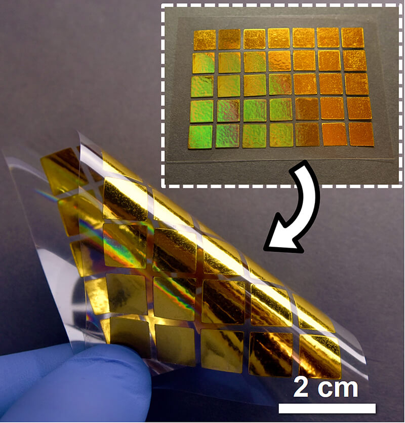
Because ultrafast, future electronics will require very small components, the stamp is designed at the nanoscale.
The technique provides a cheap method to fabricate large amounts of metallic nanostructures.
“Forming metals with increasingly smaller shapes requires molds with higher and higher definition, until you reach the nanoscale size,” Martinez said in a statement.
“Adding the latest advances in nanotechnology requires us to pattern metals in sizes that are even smaller than the grains they are made of. It’s like making a sand castle smaller than a grain of sand.”
The new technique allows researchers to get past the previous “formability limit” that made it hard to create materials with nanoscale resolution at high speeds.
It also makes metallic circuits much smoother, thus allowing electric currents to travel more efficiently with a lower risk of overheating.
For manufacturers, the technique can be easily implemented.
“Thanks to this fabrication process, many companies will be able to incorporate nanostructures to their products for different applications only by performing small modifications to the equipment they already have,” said Martinez.
A paper describing the full study is published in the journal Nano Letters.
What’s next?
The technique could eventually result in the creation of touchscreen devices that are covered in nanostructures capable of interacting with light to create 3D images.
But the most immediate objective is to “make this nanoforming process even less costly and more readily available by using inexpensive blue laser diodes,” said Martinez.
“By reducing the cost of the laser required, we will be able to make this nanopatterning technique available to a large number of users and significantly reduce the production cost of metallic nanostructures with exotic optical properties.”
It will take a significant amount of time before this technique makes an impact, but that is typical for any technology entering the industrial environments, according to Martinez.
“As soon as different industries verify the reliability of this nanofabrication technique, we will see its implementation at different scales,” he said.